|
|
| (4 intermediate revisions by the same user not shown) |
| Line 3: |
Line 3: |
|
| |
|
| ==Introduction== | | ==Introduction== |
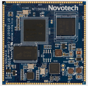
| [[File:Smart4418-SDK-1606O1.jpg|thumb|500px|Overview]] | | [[File:RK3308_CB.png|thumb|300px|Overview]] |
| [[File:Smart4418-SDK-1606F1.jpg|thumb|500px|Front]]
| | |
| ==Dimension== | | ==Dimension== |
| ::{| class="wikitable" | | ::{| class="wikitable" |
| Line 14: |
Line 14: |
|
| |
|
| ==Specifications== | | ==Specifications== |
| [[File:Smart4418-SDK-Features001.jpg|thumb|600px|Features]]
| |
|
| |
|
| ::{| class="wikitable" | | ::{| class="wikitable" |
| Line 49: |
Line 48: |
| |} | | |} |
|
| |
|
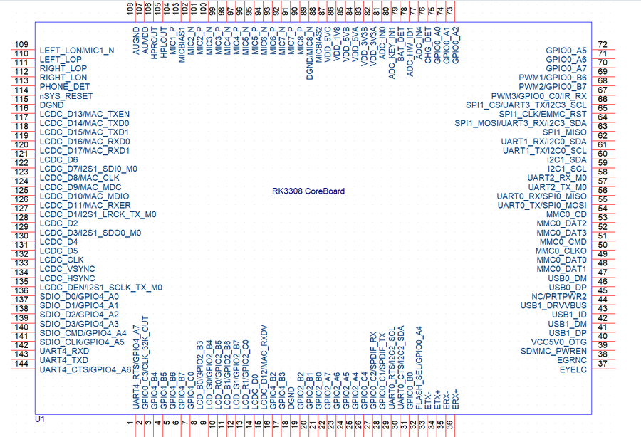
| ==Diagram, Layout and Dimension== | | ==Diagram== |
| ===Pin Descriptions=== | | ===Pin Descriptions=== |
| *'''26Pin UART/SPI/I2C/PWM Interface'''
| | [[File:RK3308_CB_layout.png|900px]] |
| ::{| class="wikitable"
| |
| |-
| |
| |Pin# || Name ||Pin# || Name
| |
| |-
| |
| |1 || VDD_3.3V ||2 || VDD_5V
| |
| |-
| |
| |3 ||I2C0_SDA ||4 || VDD_5V
| |
| |-
| |
| |5 || I2C0_SCL ||6 || DGND
| |
| |-
| |
| |7 || NC ||8 || UART3_TX
| |
| |-
| |
| |9 || DGND ||10 || UART3_RX
| |
| |-
| |
| |11 || NC ||12 || GPIOD1/PWM0
| |
| |-
| |
| |13 || NC ||14 || DGND
| |
| |-
| |
| |15 || NC ||16 || GPIOC13/PWM1
| |
| |-
| |
| |17 || VDD_3.3V ||18 ||NC
| |
| |-
| |
| |19 || SPI0_MOSI/GPIOC31 ||20 || DGND
| |
| |-
| |
| |21 || SPI0_MISO/GPIOD0 || 22 || NC
| |
| |-
| |
| |23 || SPI0_CLK/GPIOC29 || 24 || SPI0_CS/GPIOC30
| |
| |-
| |
| |25 || DGND || 26 || NC
| |
| |}
| |
| | |
| *'''LVDS Interface'''
| |
| ::{| class="wikitable"
| |
| |-
| |
| |Pin# || Name ||Pin# || Name
| |
| |-
| |
| |1 || SYS_3.3V ||2 || SYS_3.3V
| |
| |-
| |
| |3 ||GPIOC16 ||4 || GPIOB18
| |
| |-
| |
| |5 || DGND ||6 || DGND
| |
| |-
| |
| |7 || LVDS_D0- ||8 || LVDS_D0+
| |
| |-
| |
| |9 || LVDS_D1- ||10 || LVDS_D1+
| |
| |-
| |
| |11 || LVDS_D2- ||12 || LVDS_D2+
| |
| |-
| |
| |13 || DGND ||14 || DGND
| |
| |-
| |
| |15 || LVDS_CLK- ||16 || LVDS_CLK+
| |
| |-
| |
| |17 || LVDS_D3- ||18 || LVDS_D3+
| |
| |-
| |
| |19 ||I2C2_SCL ||20 || I2C2_SDA
| |
| |}
| |
| | |
| *'''DVP Camera Interface'''
| |
| ::{| class="wikitable"
| |
| |-
| |
| |Pin# || Name
| |
| |-
| |
| |1, 2 || SYS_3.3V
| |
| |-
| |
| |7,9,13,15,24 || DGND
| |
| |-
| |
| |3 || I2C0_SCL
| |
| |-
| |
| |4 || I2C0_SDA
| |
| |-
| |
| |5 || GPIOB14
| |
| |-
| |
| |6 || GPIOB16
| |
| |-
| |
| |8,10 || NC
| |
| |-
| |
| |11 || VSYNC
| |
| |-
| |
| |12 || HREF
| |
| |-
| |
| |14 || PCLK
| |
| |-
| |
| |16-23 || Data bit7-0
| |
| |}
| |
| | |
| *'''LCD Interface'''
| |
| ::{| class="wikitable"
| |
| |-
| |
| |Pin# || Name || Description
| |
| |-
| |
| |1, 2 || VDD_5V || 5V Output, it can be used to power LCD modules
| |
| |-
| |
| |11,20,29, 37,38,39,40, 45|| DGND || Ground
| |
| |-
| |
| |3-10 || Blue LSB to MSB || RGB blue
| |
| |-
| |
| |12-19 || Green LSB to MSB || RGB green
| |
| |-
| |
| |21-28 || Red LSB to MSB || RGB red
| |
| |-
| |
| |30 || GPIOB25 || available for users
| |
| |-
| |
| |31 || GPIOC15 || occupied by FriendlyARM one wire technology to recognize LCD models <br>
| |
| and control backlight and implement resistive touch, not applicable for users
| |
| |-
| |
| |32 || XnRSTOUT Form CPU || low when system is reset
| |
| |-
| |
| |33 || VDEN || signal the external LCD that data is valid on the data bus
| |
| |-
| |
| |34 || VSYNC || vertical synchronization
| |
| |-
| |
| |35 || HSYNC || horizontal synchronization
| |
| |-
| |
| |36 || LCDCLK || LCD clock, Pixel frequency
| |
| |-
| |
| |41 || I2C2_SCL || I2C2 clock signal, for capacitive touch data transmission
| |
| |-
| |
| |42 || I2C2_SDA || I2C2 data signal, for capacitive touch data transmission
| |
| |-
| |
| |43 || GPIOC16 || interrupt pin for capacitive touch, used with I2C2
| |
| |-
| |
| |44 || NC || Not connected
| |
| |}
| |
| | |
| *'''SATA Interface'''
| |
| ::* Standard 7Pin Data Interface, 4Pin Power Interface
| |
| ::[[File:SATA-01.png|frameless|500px|]]
| |
| | |
| | |
| *'''Power Interface'''
| |
| ::*DC power jack, applicable for DC 5.5 * 2.1mm power jack, DC 9V~24V/2A. When you connect a SATA hard disk or LVDS LCD to it a 12V/3A power adapter is required
| |
| ::[[File:DC-005.png|frameless|200px|]]
| |
| | |
| ::*2.54mm pitch, 2510-4P pin-header, Pin1~Pin4 description: VDD_12V, DGND, DGND, 12V_IN<br>Pin 12V_IN is connected to DC power jack, VDD_12V is connected to 12V_IN through the S1 switch
| |
| ::[[File:CON5.png]]
| |
| | |
| ===Dimensional Diagram===
| |
| [[File:Smart4418SDK-1606-Dimensions.png|frameless|800px|Smart4418SDK-1606-Dimensions]]
| |
| | |
| ::For more details refer to :[http://wiki.friendlyarm.com/wiki/images/9/90/Smart4418-1606-Dimensions%28dxf%29.zip dxf file]
| |
| | |
| ==Resources==
| |
| :SDK Carrier Board Hardware Technical Documents
| |
| ::[http://wiki.friendlyarm.com/wiki/images/c/c0/Smart4418SDK-1606-PCB%28brd%29.zip PCB source files], Allegro 16.5 or above<br>
| |
| ::[http://wiki.friendlyarm.com/wiki/images/9/90/Smart4418-1606-Dimensions%28dxf%29.zip PCB dxf file]<br>
| |
| ::[http://wiki.friendlyarm.com/wiki/images/1/1c/Smart4418SDK-1606-Schematic%28dsn%29.zip schematics], OrCAD 16.5 or above<br>
| |
| ::[http://wiki.friendlyarm.com/wiki/images/9/90/Smart4418SDK-1606-Schematic.pdf schematics in pdf]
| |
| :[http://wiki.friendlyarm.com/wiki/index.php/Smart4418 Smart4418 CPU board wiki]<br>
| |
| :[http://wiki.friendlyarm.com/wiki/images/0/0b/Smart4418-1512-Schematic.pdf Smart4418 CPU board schematics in pdf]
| |
| | |
| ==Update Log==
| |
| ===August-02-2016===
| |
| * Released English version
| |
|
| |
|
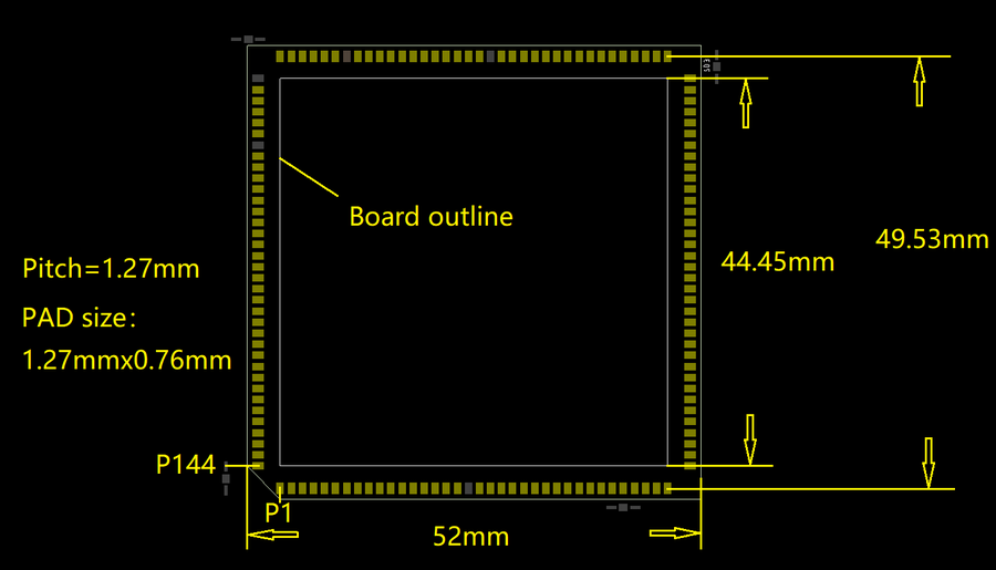
| ===Dec-08-2016=== | | ==Layout== |
| * Updated Section 2
| | [[File:Rk3308_layout.png|900px]] |


